High-resolution X-ray diffraction (HR-XRD) measurements of compound semiconductors
2023-09-16 10:00High-resolution XRD (HR-XRD) is a common method for measuring the composition and thickness of compound semiconductors such as SiGe, AlGaAs, InGaAs, etc.
When dopants or impurities are added to a single crystal lattice in a displacement manner, the lattice will strain due to the presence of doping atoms. For example, in an Si lattice, the presence of Ge atoms causes compressive strain because Ge atoms are larger than Si atoms in the lattice. This strain changes the spacing of the Si lattice, and this spacing difference can be detected by HR-XRD.

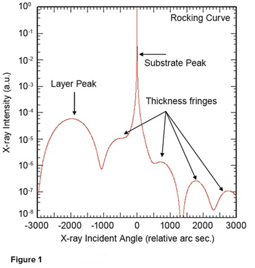
Figure 1: Theoretical HR-XRD scanning of a general structure under compressive strain, such as a 10nm SiGe layer on a Si substrate. The spikes at 0 degrees come from the Si lattice in the substrate.
The presence of larger Ge atoms causes the Si atoms in the SiGe layer to be further apart, making the diffraction peak shift to a lower Angle (to the left of the substrate peak). Because the 10nm SiGe layer is thinner, the diffraction peak of the SiGe layer is much wider than that of the Si substrate.
In such films, only a few rows of atoms with a certain arrangement can be used to produce a diffraction signal, and the X-ray diffraction peak is wider than diffraction from an Si substrate, because there are thousands of rows in the substrate that can be used to produce the atomic sequence of diffraction signals. If the structure is under tensile strain, the Si atoms will be more closely spaced than the Si atoms in the substrate, and the corresponding diffraction peak will move to the right of the substrate peak. The extra peaks in the spectrum, called "thickness streaks," come from enhanced interference of X-rays reflected by the interface between the SiGe layer and the Si substrate. This is the same signal used for X-ray reflectance (XRR) analysis and can be used to determine the thickness of the strain layer.

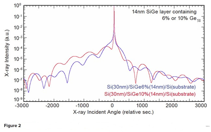
This method can be used to determine the composition of the strain layer. Figure 2 shows a theoretical HR-XRD scan of two samples, grown from a 30nm Si on a 14nm SiGe on an Si substrate. In the first case, there is 6% Ge in the lattice, while in the other case, there is 10% Ge. HR-XRD can easily tell the difference between these two structures and determine the thickness of the layer based on the thickness fringe.
In addition, advanced modeling techniques allow for accurate descriptions of structural features, such as SiGe layers with graded structures. HR-XRD can measure a variety of epitaxial materials, such as AlGaAs, InGaAs, InGaN, etc. Generally, XRD can determine the composition of these thin film layers with an accuracy of less than 1%. However, it should be noted that HR-XRD assumes that all doping atoms are present in the lattice.
