
Two dimensional metallic alloy contact with adjustable work function
2023-11-03 10:00Two-dimensional (2D) transition metal chalcogenides (TMDs) have attracted interest in the development of novel electronic devices due to their atomic thickness and suspension-free bond surfaces. In order to explore potential applications, it is important to be able to precisely control the chemical composition and electronic structure of 2D TMDs and their heterojunctions. Heterojunctions constructed using two-dimensional semiconductor TMDs can be used to manufacture next-generation electronic devices. However, their performance is limited by low-quality metal-semiconductor contacts, and it remains challenging to manufacture contacts with variable work functions using metallic or gold-attribute TMDs.
In this study, the authors show that a one-step chemical vapor deposition (CVD) method can be used to prepare nanosheets of a two-dimensional gold attribute alloy VS2xSe2(1-x) (where 0 ≤ x ≤ 1) with continuously adjustable band alignment. The work function of the alloy can vary from 4.79±0.01 eV (VSe2, x = 0) to 4.64±0.01 eV (VS2, x = 1.00). Van der Waals heterojunctions of VS2xSe2(1-x) and P-type WSe2 exhibit increased contact potential differences when x changes from 0 to 1, and transistors made using VSe2/WSe2 contacts show lower potential differences and better device performance than VSSe/WSe2 contacts. In both cases, Achieves better performance than devices with evaporated metal contact. The contact potential difference between the alloy and the N-type MoS2 heterojunction can range from -71.5 mV (VSe2) to 0 mV (VSSe) to 59.3 mV (VS2), that is, from Schottky contact to ohmic contact, with the lowest work function (VS2) transistor showing the best performance. Therefore, this research method provides a way to systematically modulate the work function of two-dimensional gold TMDs and band alignment of metal-semiconductor van der Waals heterojunctions grown by CVD.
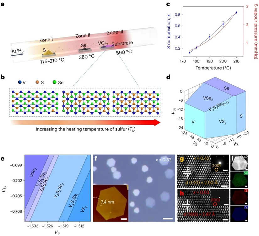
FIG.1 Synthesis and regulation of VS2xSe2(1-x) alloy nanosheets
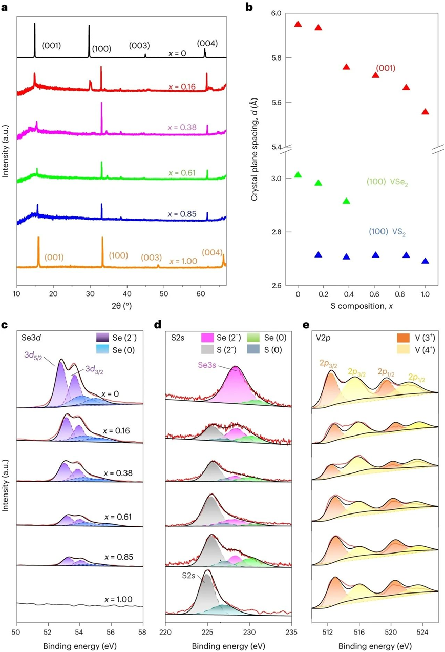
Fig.2 X-ray diffraction (XRD) and X-ray photoelectron spectroscopy (XPS) characterization of VS2xSe2(1-x) in different S-components
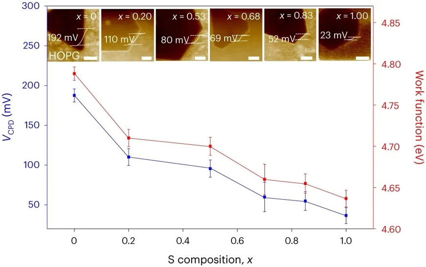
Fig 3 Kelvin Probe Force microscopy (KPFM) properties of VS2xSe2(1-x) grown on highly oriented pyrolytic graphite (HOPG)
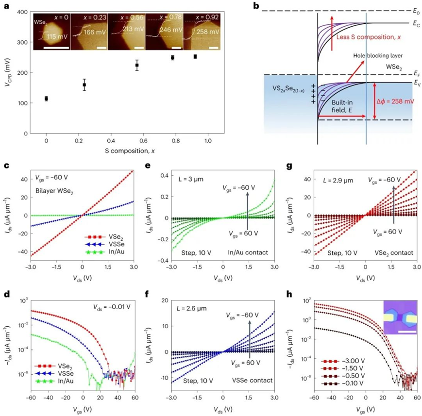
Fig4 KPFM measurements and electrical properties of VS2xSe2(1-x)/WSe2 van der Waals heterojunction field-effect transistors (FETs)
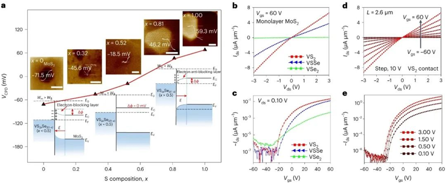
FIG. 5 KPFM and electrical properties of VS2xSe2(1-x)/MoS2 van der Waals heterojunction FETs
