Crystal defect - Dislocation
2023-10-22 10:00Elemental extremely low temperature superconductors can be understood as: the ideal lattice should be at absolute zero to achieve lattice vibration zero. Because it is not "ideal", the lattice vibration is achieved at a higher temperature above absolute zero. To investigate the reasons, the first thing that comes to mind is that there are crystal defectsand layer faults in this kind of elemental crystals. Because in this kind of metal crystal, other more powerful lattice states are no longer available, so that the effect of this crystal line defect and plane defect on the lattice is fully displayed.
In addition to the different types of spot defects, there are two major types of crystal defects: one fault and layer fault. This is also one of the important research fields of metallography and crystallography in modern times. Dislocation can be divided into edge dislocation and screw dislocation. No matter what kind of dislocation, it has an important effect on the physical properties of crystal materials.
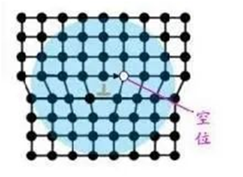
1. Edge dislocation See figure

There is a dark edge dislocation symbol "⊥" in the middle area, which is the edge dislocation position, the dislocation line vertical plane, the atomic plane (or crystal plane) slide direction vertical dislocation line. The circular blue region indicates the range of influence of dislocation stress, that is, the range of lattice distortion. In the distance the lattice returns to normal. The atomic sheet (two-dimensional lattice) at the dislocation line is like a knife blade, and the crystal face is suddenly faulted.
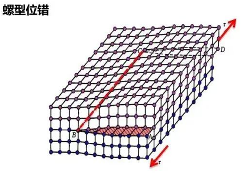
2. Screw dislocation diagram

The line is the location of the dislocation line, and the slip plane painted in red is the dislocation plane. The glide direction is parallel to the direction of the dislocation line. Looking in the direction of the dislocation line, the spiral dislocation is equivalent to the crystal face rising around an axis at a lattice spacing. The continuous lattice distortion near the dislocation line results in microscopic stress. It'll recover a little bit later. The two kinds of dislocations have the properties of moving, recombination, pinning and aggregation to form small corner grain boundaries.
