
Application of XRD technology in semiconductor industry
2023-09-20 10:00Global semiconductor equipment spending has entered an upward cycle. The application of new technologies and new products such as 5G, Internet of Things, big data, artificial intelligence and automotive electronics will bring huge semiconductor market demand, and the industry will enter a new round of rising cycle. Wafer production, epitaxial growth, packaging and integration at the front end of the entire industry chain, and its process and product quality are directly related to downstream industry applications. Rigaku has a complete system of equipment, such as X-ray diffraction (XRD), X-ray fluorescence (XRF), X-ray reflectometer (XRR) and X-ray topography (XRT), which can be applied to the whole process from wafer production to integrated circuits, and can non-destructive measurement of a number of key process parameters: Such as thickness, composition, roughness, density, porosity, as well as crystal structure and crystal structure defects.
1. In wafer production, the number and type of defects will greatly affect the subsequent steps. X-ray topological imaging (XRT) can clearly observe defects and dislocations on the wafer surface (Figure 1). Help producers to improve the process and control the quality.
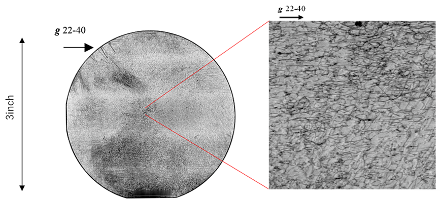
Figure 1: Transmission topology imaging of a 4H-sic wafer
2. The uniformity of wafer or epitaxial film can be measured by XRD swing curve function, and the visualization software module provided by Rigaku can also give two-dimensional distribution images, which can intuitively evaluate the quality of the surface (Figure 2).
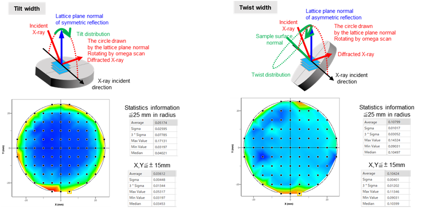
Figure 2: Two-dimensional image of AlN film growing on sapphire substrate
3. The thickness of the film can be measured by a high-resolution swing curve, which is non-destructive and highly accurate (Figure 3).
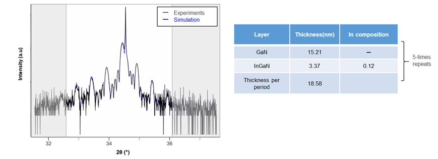
Figure 3: High-resolution swing curve for measuring the thickness of GaN/InxGa(1-x)N films
4. There may be some kind of lattice mismatch during wafer or epitaxial film growth, which will affect the quality of the film. Using Rigaku's special detectors and solutions, reciprocal space testing can be done on SmartLab, where lattice mismatches and crystallographic constants can be seen very intuitively.
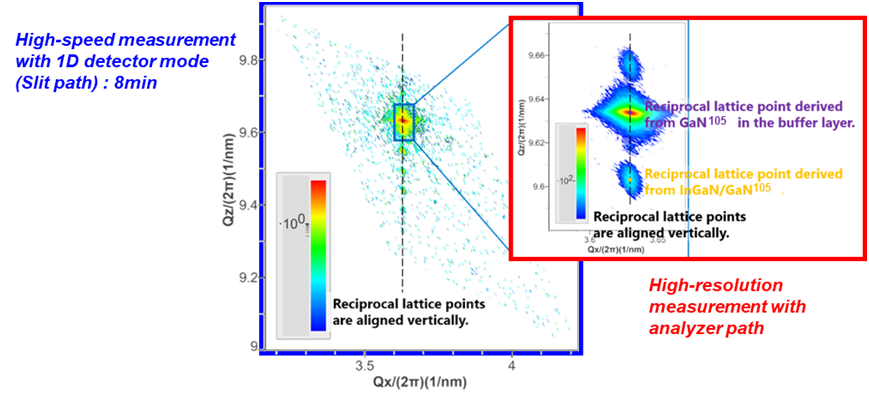
Figure 4: high-resolution reciprocal spatial spectrum of GaN105
